BDF
Via and Fine-Interconnect Etching for Advanced Packaging
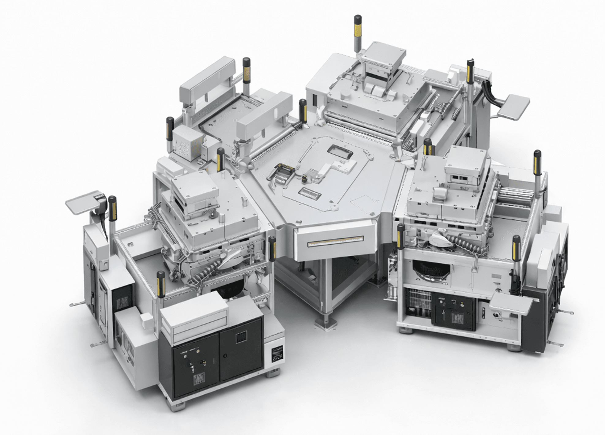
A plasma etch platform for BDF via formation and residue removal in semiconductor glass substrates and advanced packaging.
Combines high productivity and etch rate with precise C/D control and within/across uniformity.
Core technology
- High throughput and high etch rate
- Excellent within / across uniformity
- High MTBF and optimized PM cycle
- Low particle defect and high uptime
Applications
- BDF Via-Hole Plasma Drilling
- Post-Drill Desmear
- Post-Develop Descum
Target applications
Glass Interposer / PLP