SEMICONDUCTOR · DISPLAY · ADVANCED PACKAGEICD BRAND FILM · 50 SECICD BRAND FILM · 30 SEC

PRECISION IN THE INVISIBLE

WORLD FIRST,ETCHED BYICD.

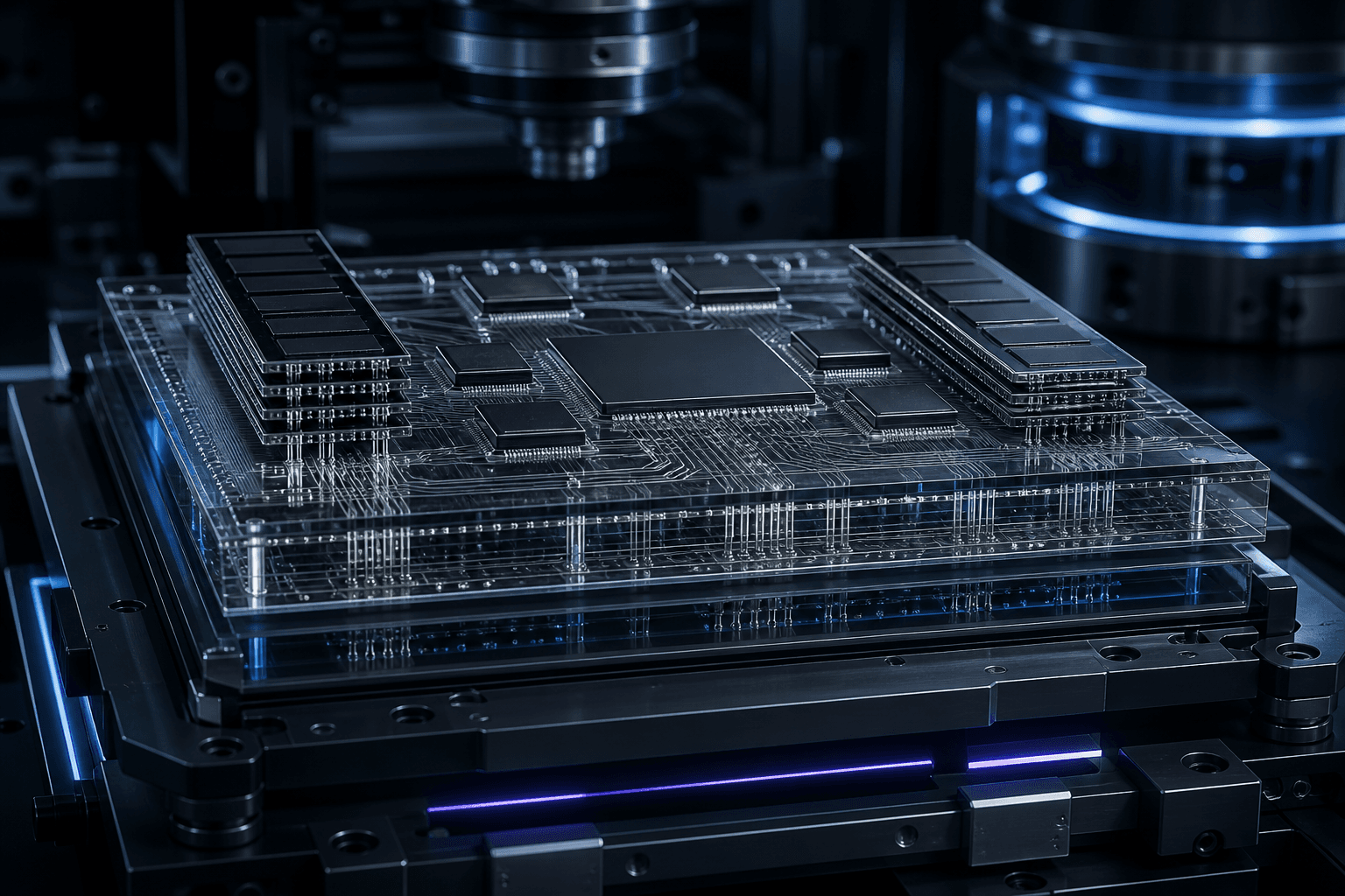
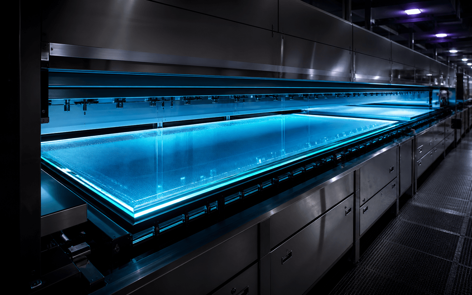
From the world-first CiM to large-area etch proven in OLED production, ICD turns processes no one has built before into standards ready for semiconductor, packaging and display manufacturing.

Discover ICD’s precision plasma systems.
SEMICONDUCTOR & DISPLAY ETCH SYSTEMS

EQUIPMENT PORTFOLIO

ETCH TECHNOLOGY,PROVEN IN SYSTEMS.

Explore production-proven systems spanning advanced packaging, semiconductor front-end and display manufacturing.

View equipment details
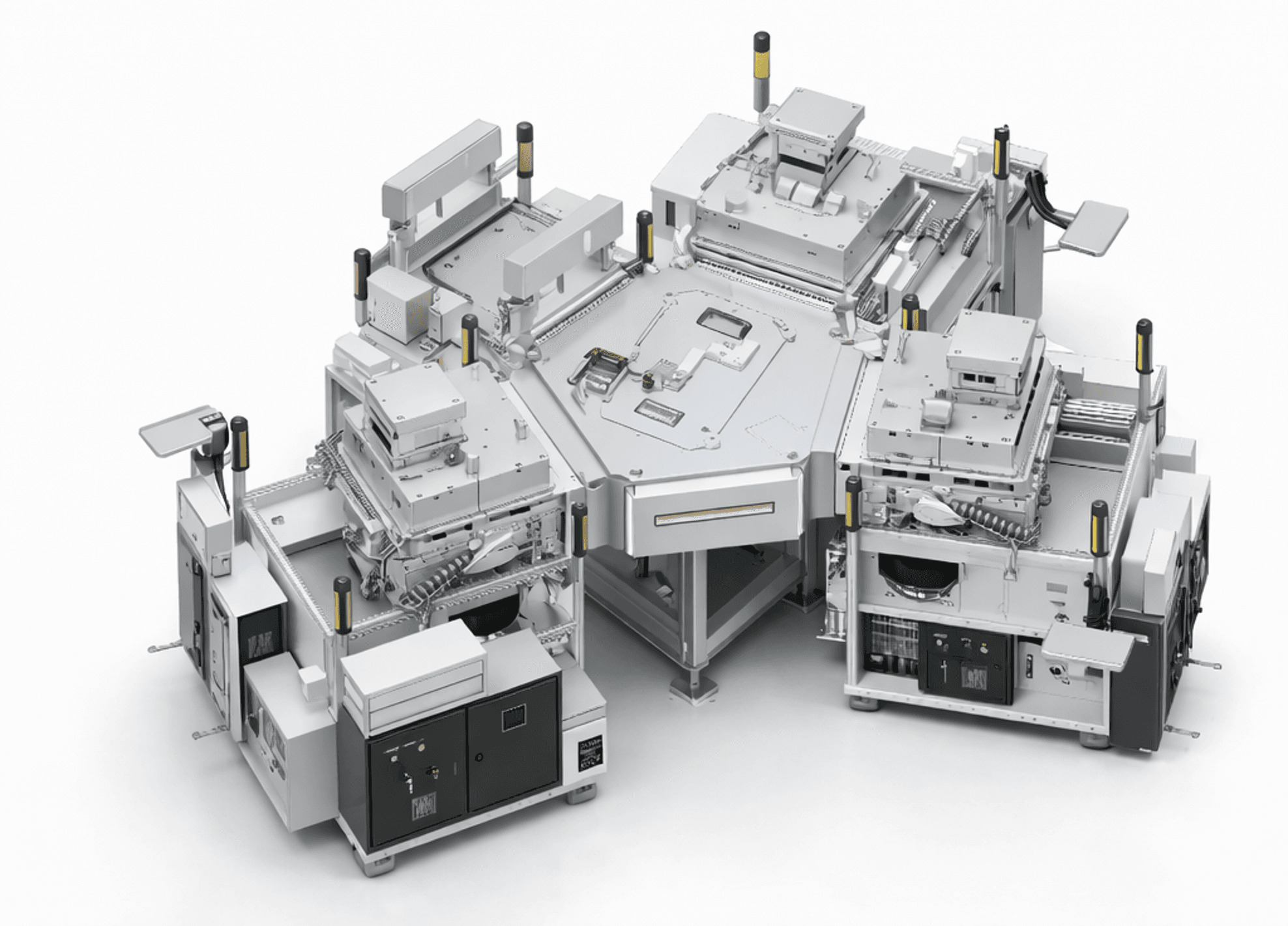
BDF Etcher equipment
PROCESSVia-hole plasma drillingPRODUCTIVITYHigh throughputUNIFORMITYWithin / across substrate
0108
Discover ICD technology
02WHAT WE ENGINEER

We create etch processes
the world has never seen.

More than 25 years of OLED production experience converge with proprietary plasma engineering. By integrating source, chamber, ESC and recipe, ICD delivers etch outcomes that are distinctly its own.

03EQUIPMENT ARCHITECTURE

From semiconductor to display.
One ICD etch standard.

Explore proprietary ICD platforms engineered to turn world-first processes into production reality.

BDF Etcher equipment
ADVANCED PACKAGING

BDF Etcher

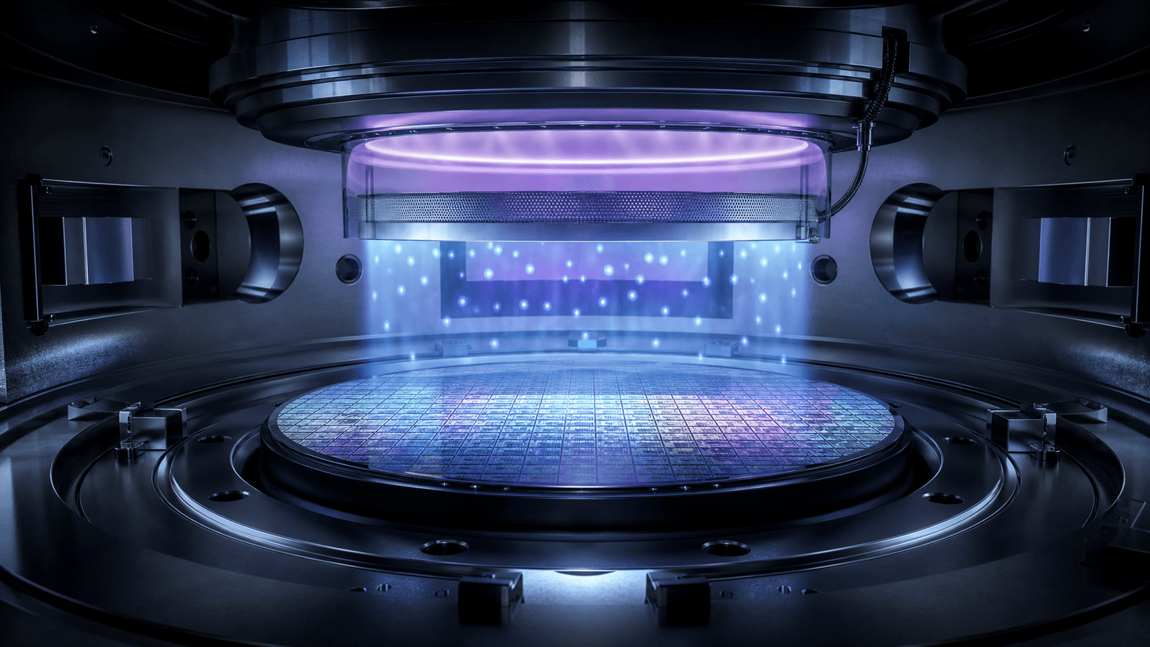
Via and Fine-Interconnect Etching for Advanced Packaging

Plasma processing for BDF vias and fine-pitch RDL

PROCESS
Via-hole plasma drilling
UNIFORMITY
Within / across substrate
PRODUCTIVITY
High throughput
BDF Via-Hole Plasma DrillingPost-Drill DesmearPost-Develop Descum
View system details
01 / 03
04PROCESS CAPABILITY MATRIX

Plasma expertise proven in display production, extended into semiconductor front-end and glass interposer processes.

HYBRID ASHING process visualization
PROCESS / RPS + RIE
RPS + RIE

HYBRID ASHING

Hybrid ashing engineered for throughput and Low-k protection

  • PULSED RADICAL SOURCE
  • INDEPENDENT RADICAL / ION CONTROL
  • WIDE PROCESS WINDOW
05INSIDE THE PROCESS

Four precision controls
that make firsts possible.

Independent command of plasma, vacuum, ion energy and temperature creates process results that are difficult to replicate.

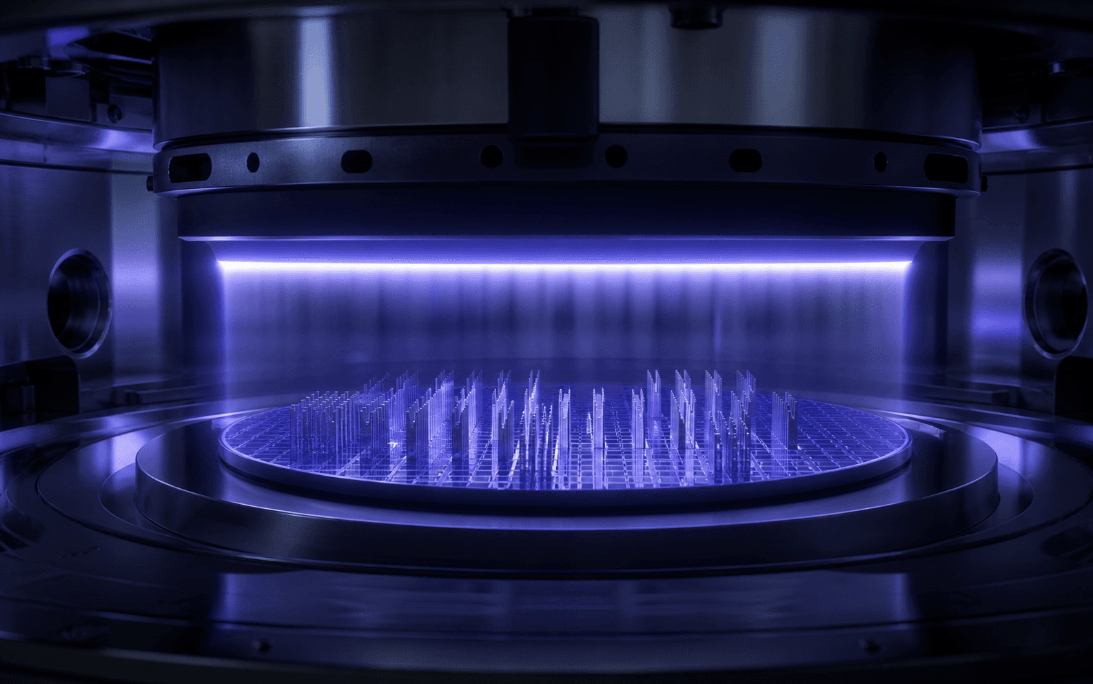
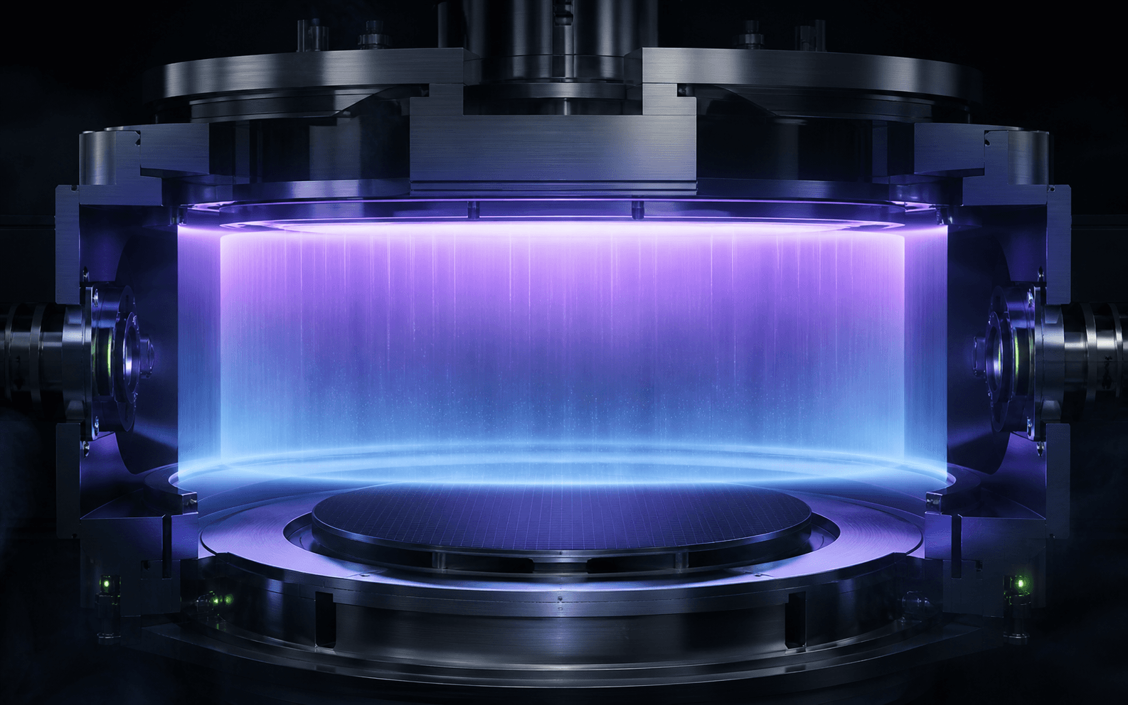
High-density, low-damage plasma process visualization
DENSITY10¹¹ cm⁻³1011cm−3 LIVE CONTROL
01 / 04PLASMA SOURCE13.56 MHz
PLASMA SOURCE / CONTROL NOTE

A proprietary source forms uniform high-density plasma across the wafer while limiting process damage.

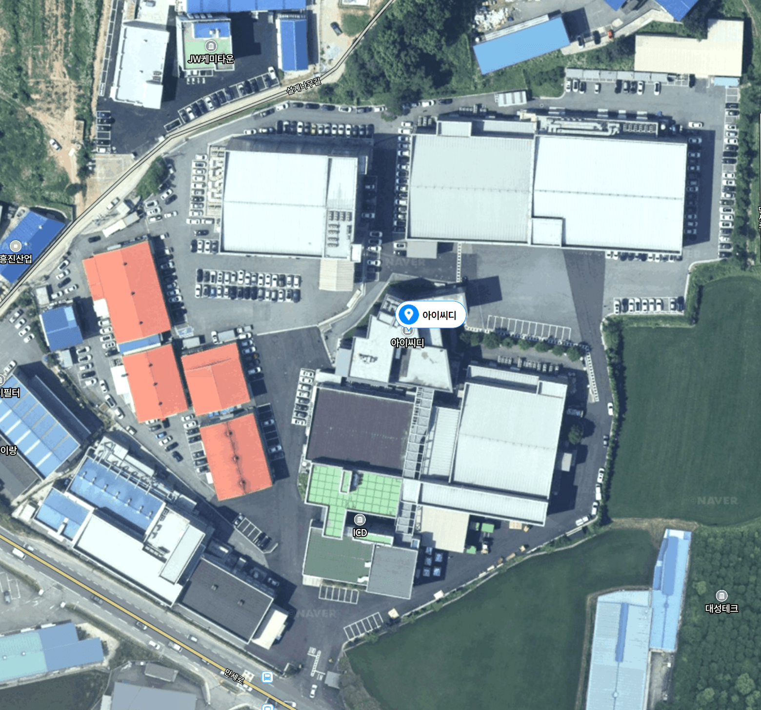
ICD Anseong engineering campus
ANSEONG · KOREA37°00'N / 127°16'E
06PROVEN IN PRODUCTION

World-first ideas.
Singular production answers.

At our integrated Anseong campus, plasma source, process, mechanical and control teams develop as one. ICD's relentless loop between design and field validation sets a new benchmark for etch.

25+Years serving OLED production
900+Production chambers
4Integrated disciplines
Explore ICD engineering
GLOBAL ETCH NETWORK

World-first engineering. Close to production.

From Anseong to customer fabs worldwide, one ICD team protects the process precision that makes every singular etch result possible.

12CUSTOMER HQ
05CONNECTED MARKETS
24/7FIELD RESPONSE
ICD GLOBAL CUSTOMER NETWORKWORLD FIRSTS · CONNECTED BY ICD

All continents and our key customer network.

● CONNECTED COUNTRYYOUR PRODUCTION SUCCESS, ALWAYS FIRST.
CUSTOMER NETWORK

Connected with innovators worldwide.

From display to advanced packaging, ICD technology connects with customer sites worldwide.