01
Dry Etch
Dry Etch Advanced ESC
| Process | Metal / Non-Metal |
|---|---|
| Cooling | +30% (vs. Conventional) |
| Generation | Up to Gen 8.6 |
| ESC Type | Unipolar |
MATERIALS · SURFACE TREATMENT · COMPONENTS
Display AMOLED ESC Technology & Product Portfolio
ESC products optimized for AMOLED etching, evaporation and thin-film processes
Dry Etch
| Process | Metal / Non-Metal |
|---|---|
| Cooling | +30% (vs. Conventional) |
| Generation | Up to Gen 8.6 |
| ESC Type | Unipolar |
PVD / Sputtering
| Process | Sputter / PVD |
|---|---|
| Function | GLS Slip / Cooling |
| Generation | Up to Gen 8.6 |
| ESC Type | Bipolar |
CVD Process
| Process | CVD |
|---|---|
| Max. Temperature | Up to 300 ℃ |
| RF Power | ~ 0.6 W/cm² |
| ESC Type | Bipolar |
Evaporation (OLED)
| Process | Evaporation (OLED) |
|---|---|
| Flatness Control | ≤ 50 ㎛ |
| Generation | Up to Gen 8.6-h |
| ESC Type | Bipolar |
Semiconductor ESC Technology & Product Portfolio
Process-temperature-optimized ESC products with Multi-Zone temperature control
PVD / Sputter / Etch
−40 ℃ ~ 20 ℃
PVD / Sputter / Etch
20 ℃ ~ 80 ℃
Metal Deposition / Metal Etch
80 ℃ ~ 150 ℃
CVD / High Temp Process
150 ℃ ~
Temperature uniformity by ESC structure

On smaller screens, scroll the diagram horizontally or open the full-size image to zoom in.
ICD Materials was established on June 1, 2018 through a physical spin-off from ICD, primarily to manufacture and sell electrostatic chuck (ESC) equipment for AMOLED and LCD equipment. Its headquarters and factory are located in Daedeok-myeon, Anseong-si, Gyeonggi-do, Korea.
The company was certified as a venture enterprise by the Small and Medium Business Administration under Article 25 of the Act on Special Measures for the Promotion of Venture Businesses.
On smaller screens, scroll the diagram horizontally or open the full-size image to zoom in.
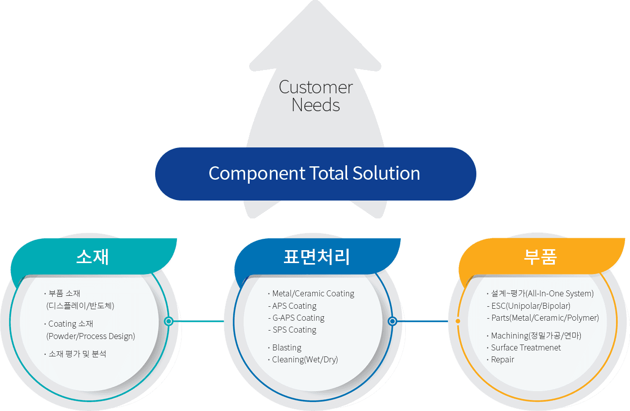
Component Total Solution: materials, surface treatment and components
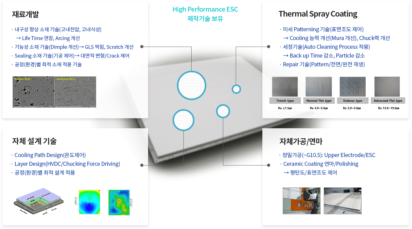
Material development, in-house design, thermal spray coating, machining and polishing
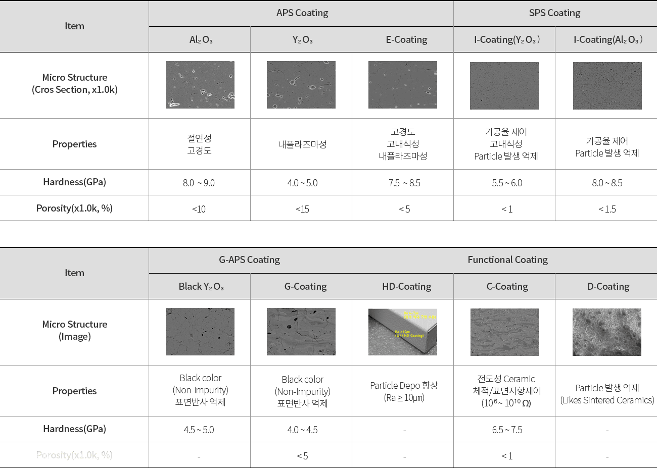
Microstructure and property comparisons for APS, SPS, G-APS and functional coatings