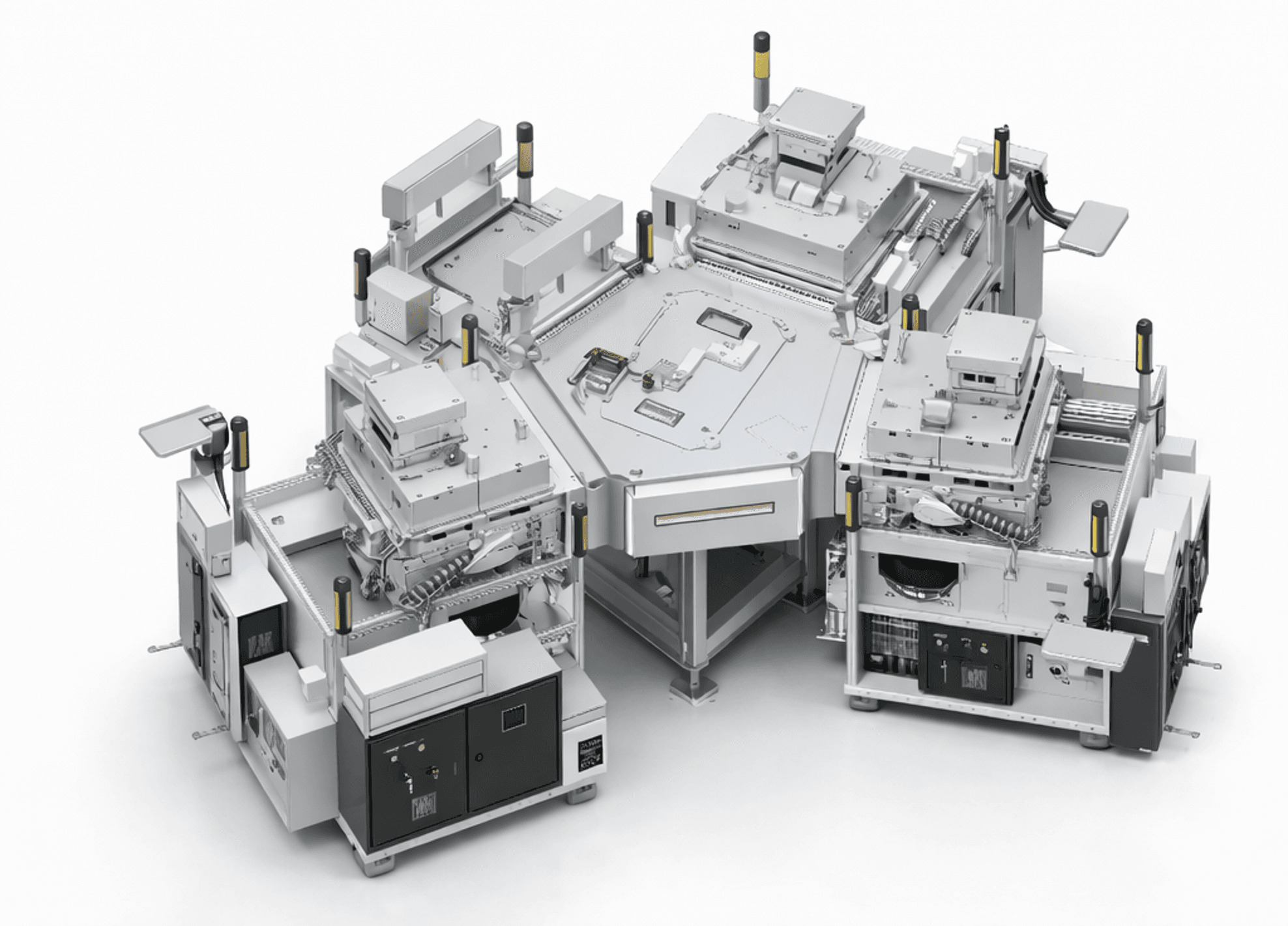
BDF
Via and Fine-Interconnect Etching for Advanced Packaging
View details↗Explore the proprietary Equipment & Technology technology and production platforms behind ICD world firsts.
Explain the plasma source, control mechanism and core technology.
→Show how the technology solves yield, productivity and quality challenges.
→Connect each process need to the right ICD platform and equipment.
Explore each product family and its purpose. Open a product for detailed technical information.
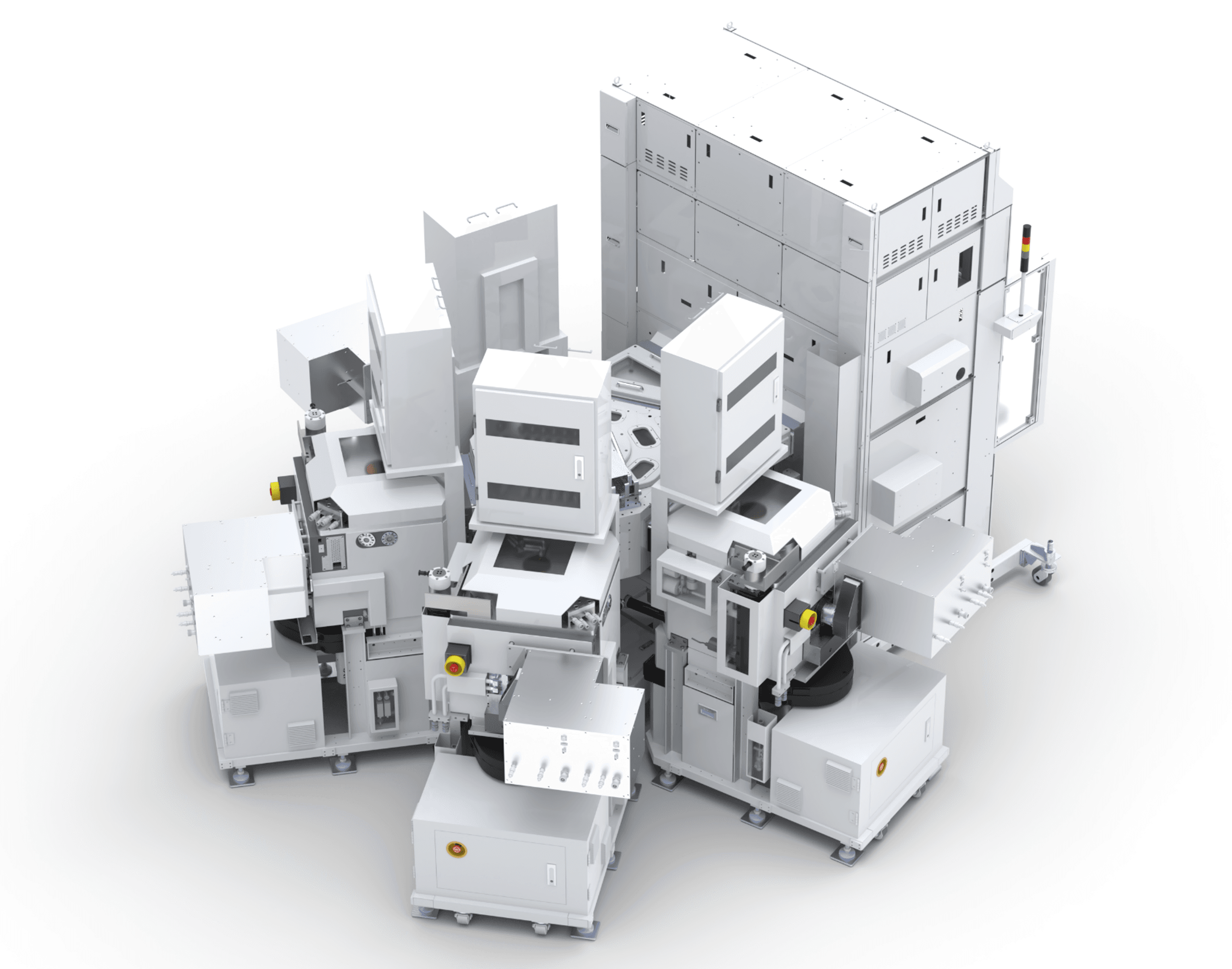
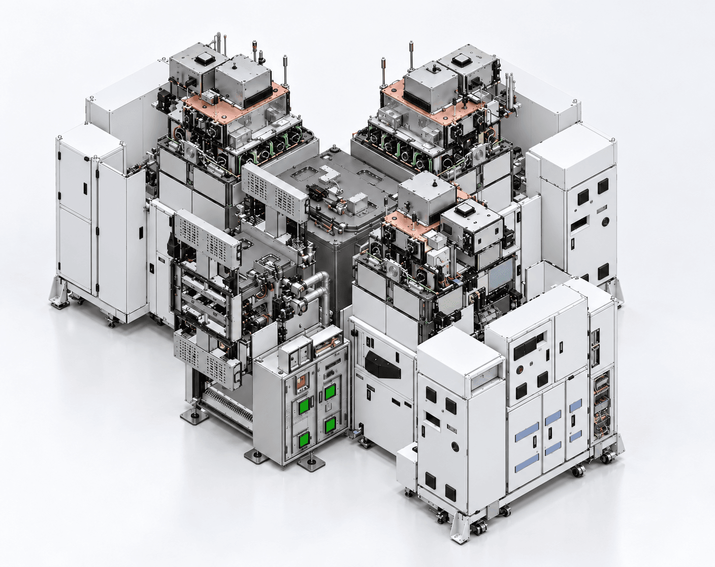
Systems for fine-interconnect processing and dielectric film deposition in advanced packaging.
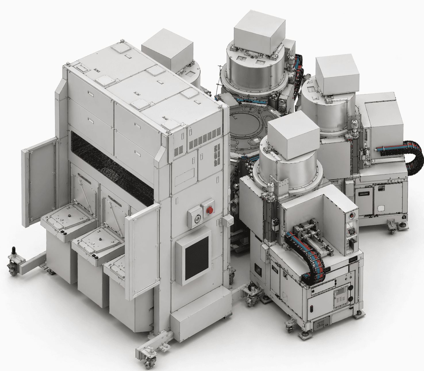
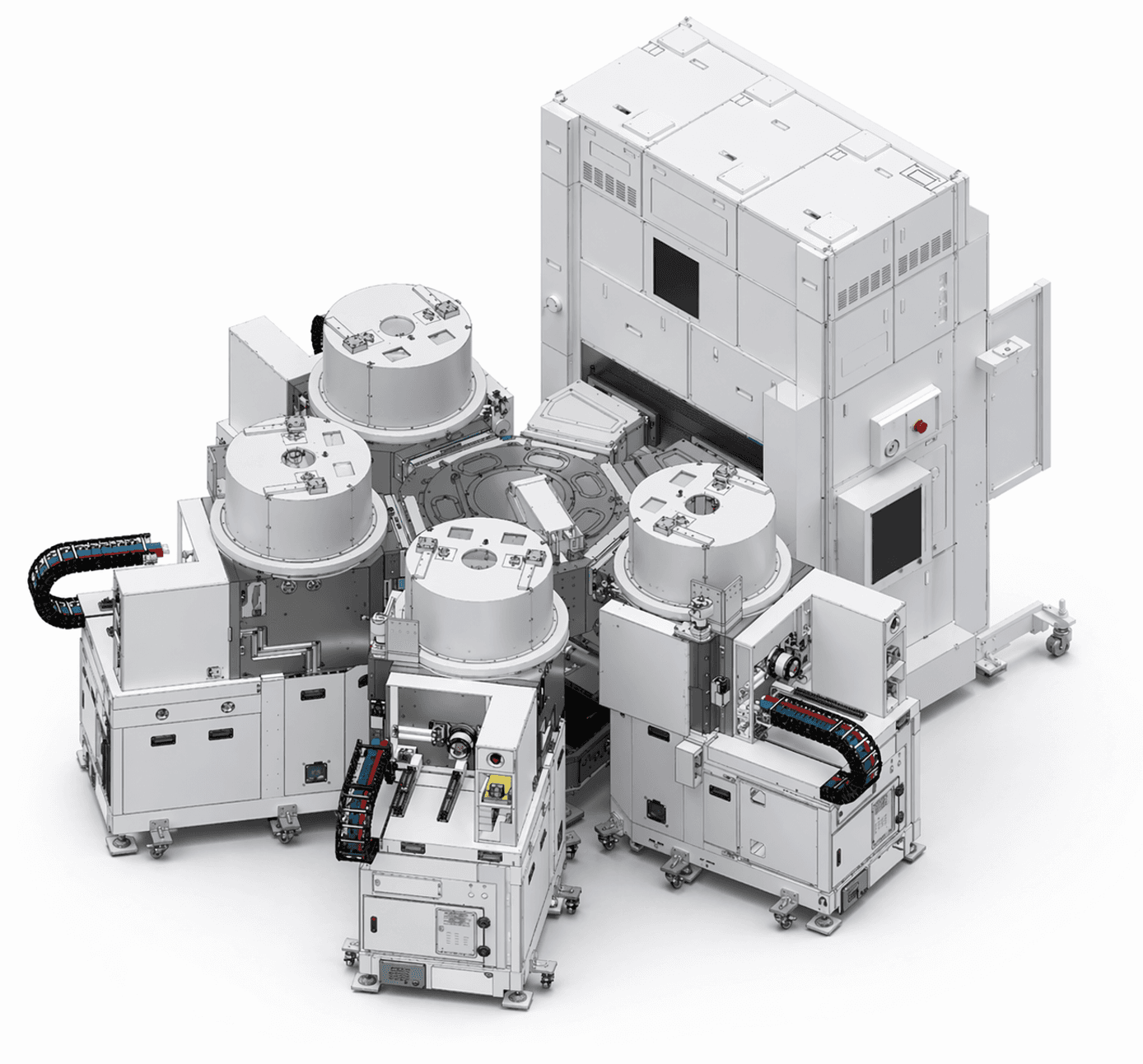
Precision wafer etching, photoresist stripping and residue removal.
Display pattern etching, pre-evaporation treatment, vacuum transfer and research deposition.
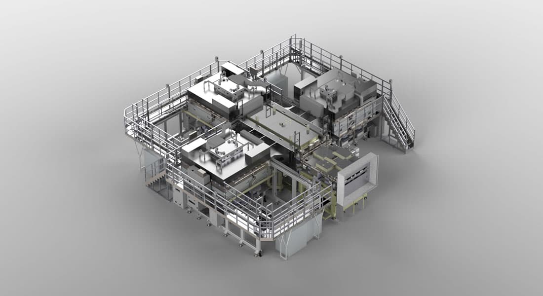
Display Pattern Etching for OLED and LCD
View details↗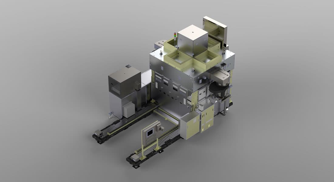
Plasma Treatment Before OLED Evaporation
View details↗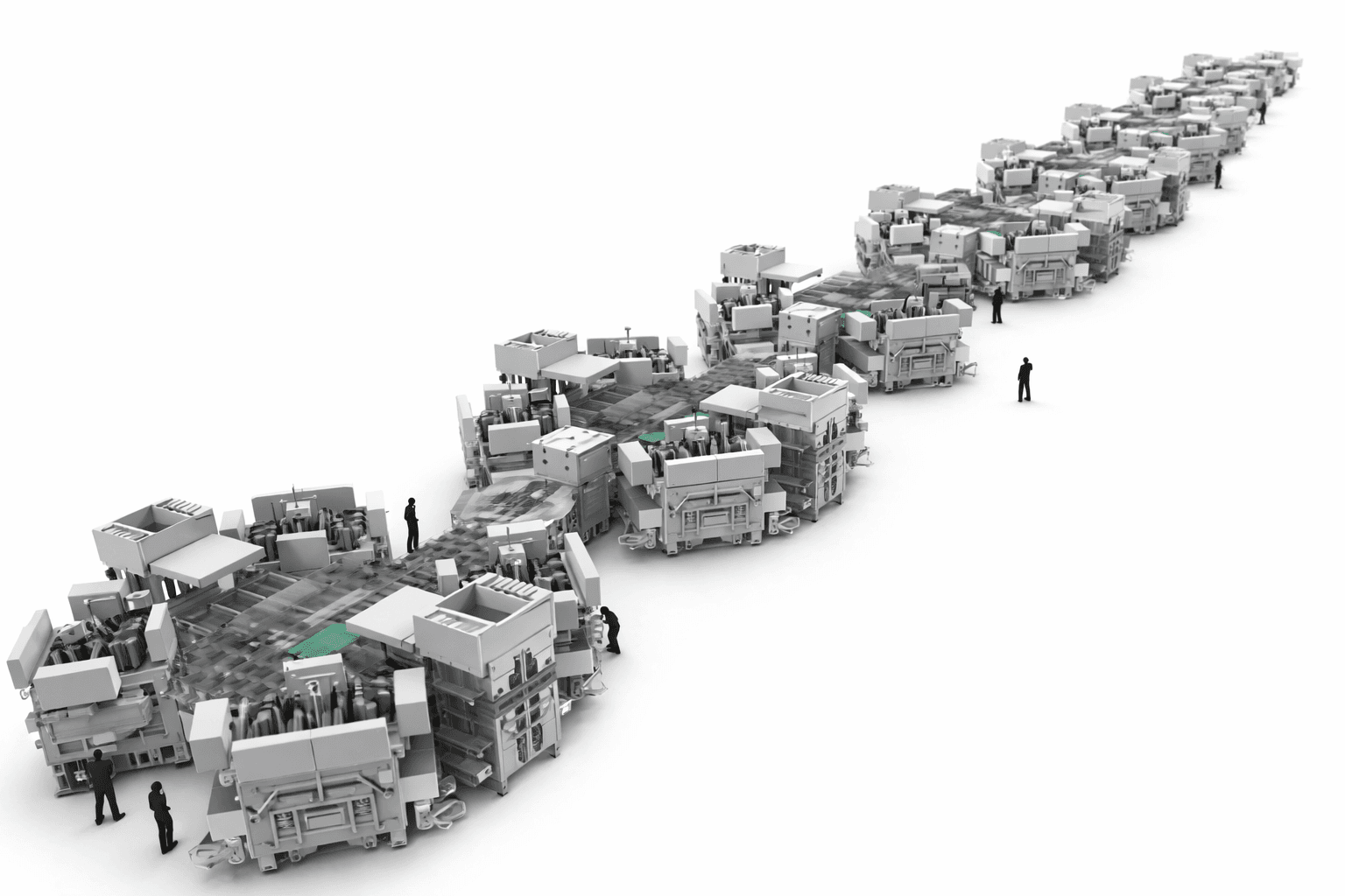
In-Line Vacuum Transfer System
View details↗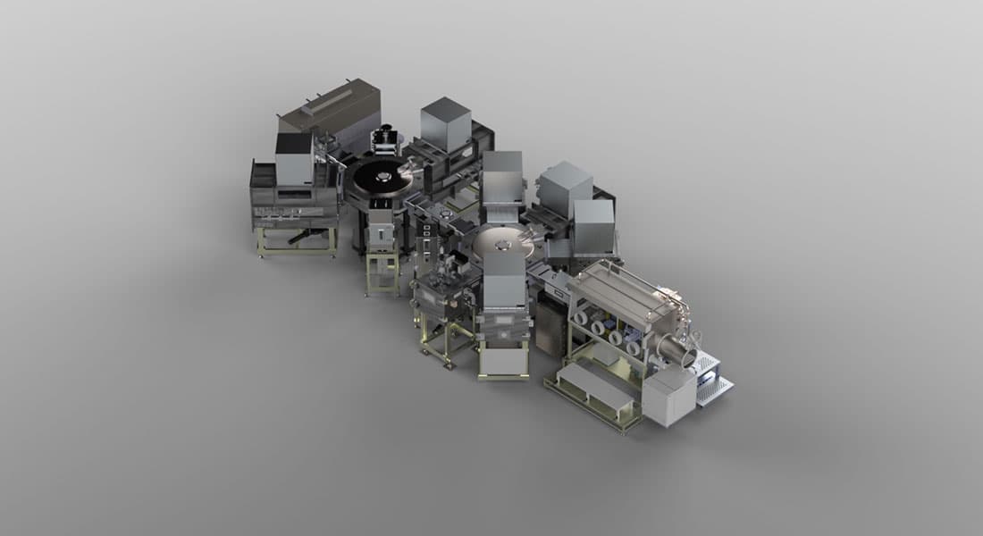
Organic and Metal Film Deposition for OLED Research
View details↗Electrostatic chucks for substrate clamping and temperature control across process applications.