HOME/장비·기술/반도체 장비
장비·기술

반도체 장비

세계 최초를 만드는 ICD의 반도체 장비 기술, 독자 공정과 양산 장비를 확인합니다.

ICD / LEADERSHIP

경영진 소개

SEMICONDUCTOR EQUIPMENT

Two equipment groups. One semiconductor growth axis.

Choose Advanced Package or Front End to explore equipment, core technologies and production applications.

ADVANCED PACKAGE

An equipment portfolio connecting fine patterning, cleaning, etch and bonding processes.

장비 포트폴리오

Explore equipment by process challenge.

Select a product to see its core principle, enabling technologies and applications in one view.

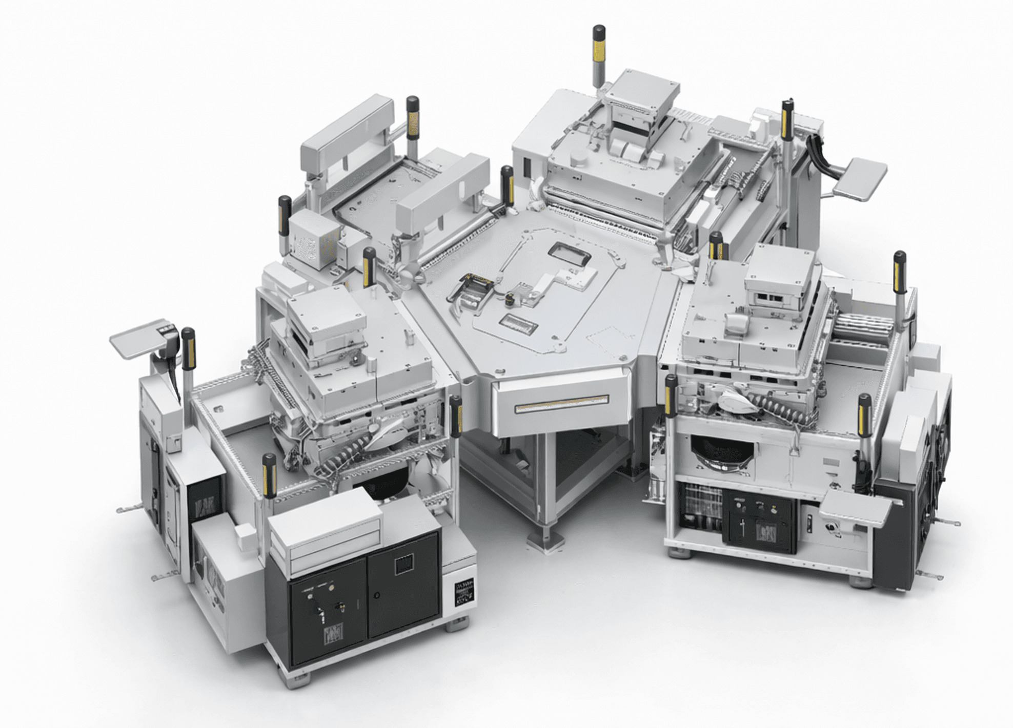
BDF equipment

BDF

Via and Fine-Interconnect Etching for Advanced Packaging

A plasma etch platform for BDF via formation and residue removal in semiconductor glass substrates and advanced packaging.

Combines high productivity and etch rate with precise C/D control and within/across uniformity.

01

Core technology

  • High throughput and high etch rate
  • Excellent within / across uniformity
  • High MTBF and optimized PM cycle
  • Low particle defect and high uptime
02

Applications

  • BDF Via-Hole Plasma Drilling
  • Post-Drill Desmear
  • Post-Develop Descum
03

Target applications

Glass Interposer / PLP