BDF
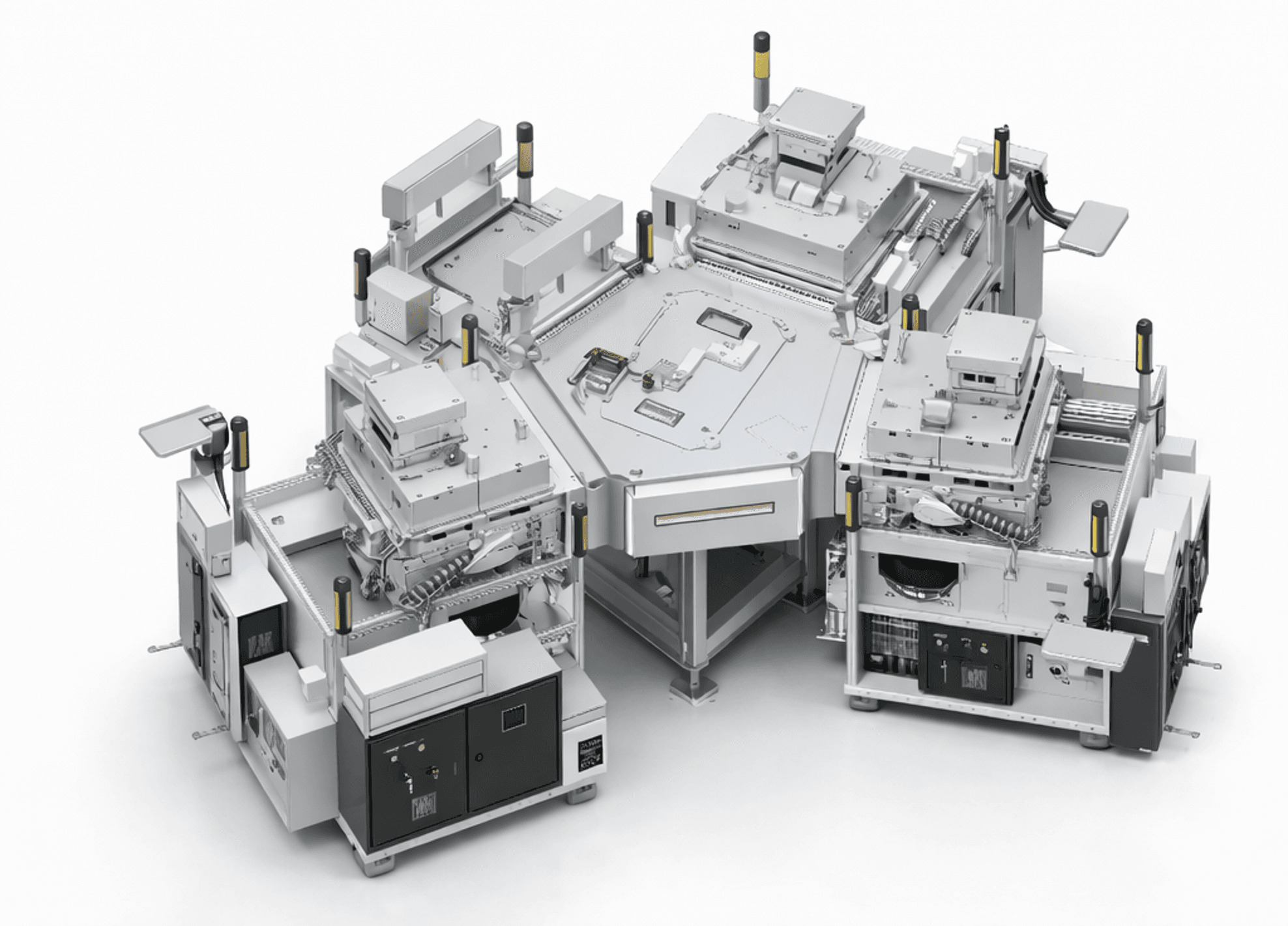
Via and Fine-Interconnect Etching for Advanced Packaging
詳細を見る↗ICDの世界初を支える装置・技術独自技術、プロセス、量産装置をご覧ください。
製品群ごとに装置と用途をご覧ください。詳しい技術情報は各製品で確認できます。
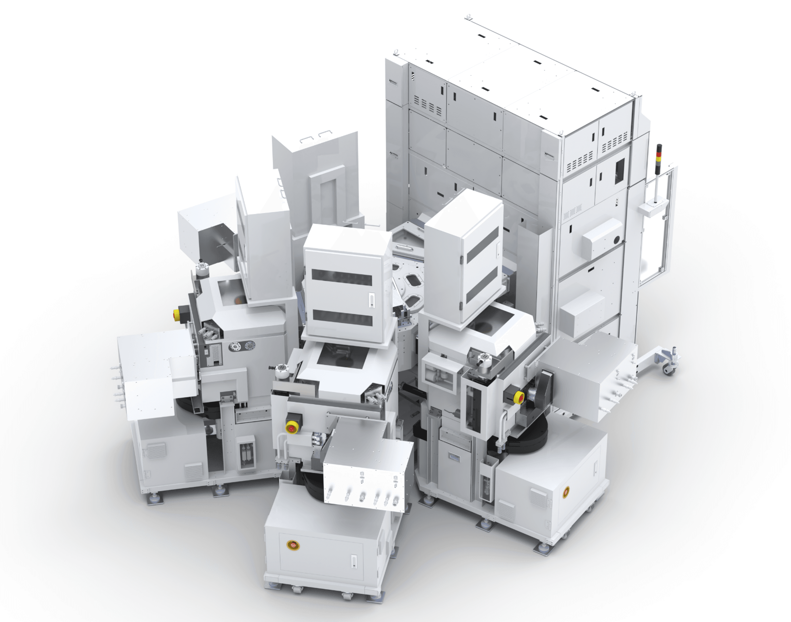
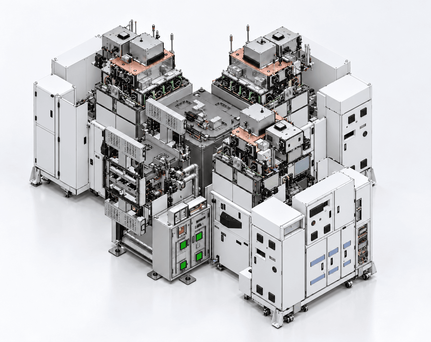
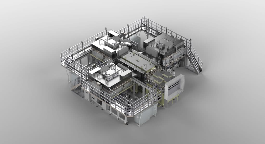
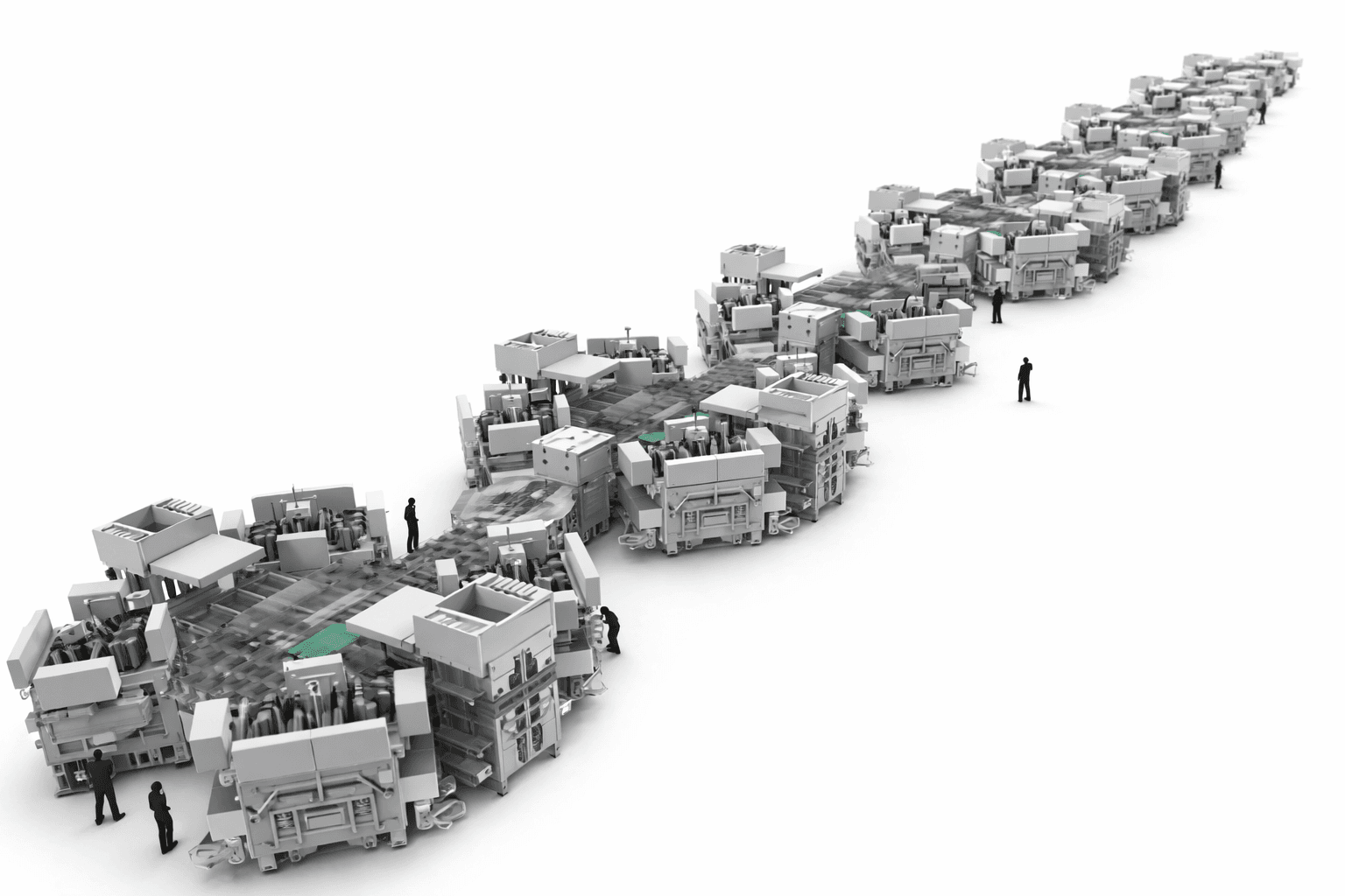
Systems for fine-interconnect processing and dielectric film deposition in advanced packaging.
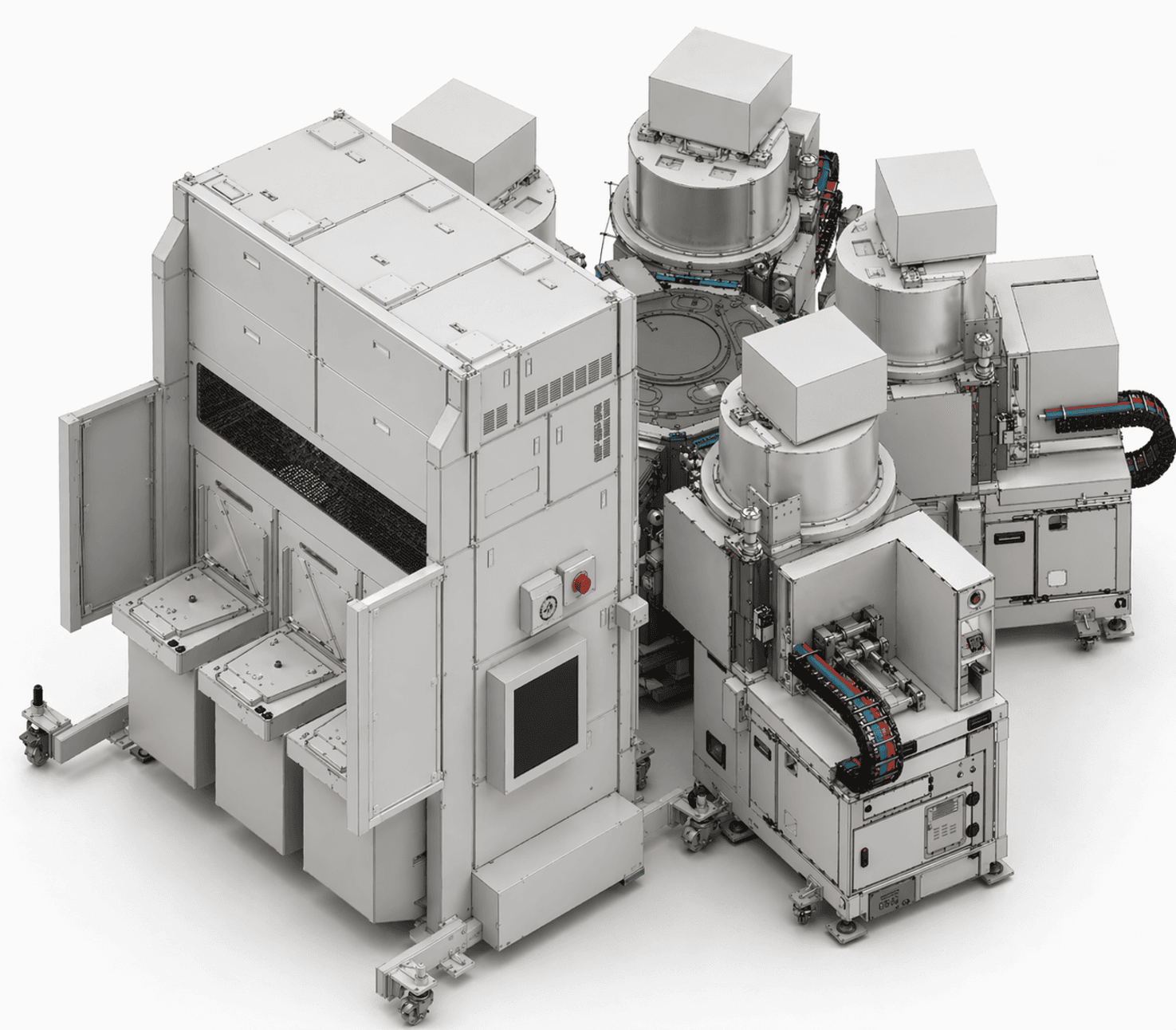
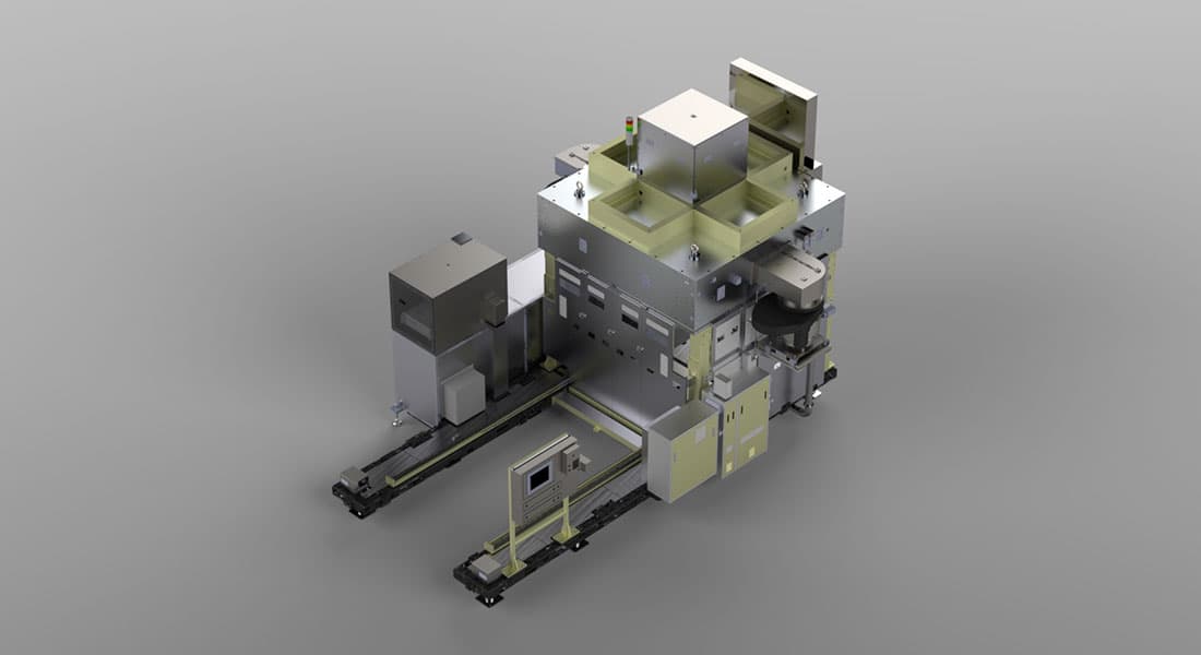
Precision wafer etching, photoresist stripping and residue removal.
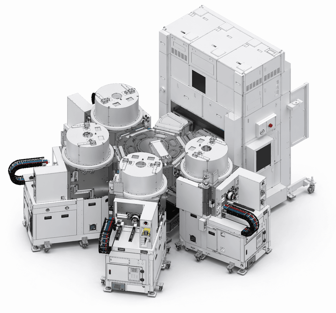
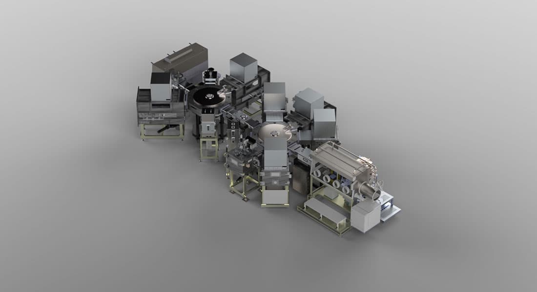
Display pattern etching, pre-evaporation treatment, vacuum transfer and research deposition.
Electrostatic chucks for substrate clamping and temperature control across process applications.